 The XCircuit Schematic Capture Tutorial
Table of Contents
- Getting Started
- Task1 Acquaint yourself with XCircuit
- Task2 Run the program
- Task3 Drawing a circuit for SPICE simulation
- Task4 Introduction to parameters
- Task5 Drawing a circuit with parameters
- Task6 Making a new "fundamental" object
- Task7 A schematic with symbol-less schematics
in the hierarchy
- Task8 Identifying electrical connections
- Task9 A symbol on its own schematic
- Task10 "sim" format and flattened
- Task11 "pcb" type netlists
- Task12 Multiple-gate chips in PCB netlists
- Task13 Modifying netlist formats
- Task14 Example: A bridge rectifier for a PCB
This tutorial is provided to help users get up and running with the
schematic capture capabilities of xcircuit.
In order to get the most out of this page, you should have already
downloaded, compiled, and installed the xcircuit program and its libraries,
and xcircuit should be compiled with schematic capture capability (on by
default; see the Imakefile for details).
IMPORTANT NOTICE:
It is necessary for you to have the new (version 2.3.3) distribution of xcircuit
compiled and installed to get the correct behavior in the tutorial.
In particular, the PostScript prolog has changed and if the old one is
prepended to the new xcircuit files, the files will not be printable or
viewable from a PostScript previewer.
There are additional differences between versions 2.1(beta) to version 2.3.3,
mainly in the way symbols and schematics are associated with each other.
The new methods are incorporated into this tutorial. Version 2.3.3 also
corrects some errors in netlist generation, and is generally more stable.
Versions before 2.3.3 will not produce pcb-style netlists
as featured in this tutorial.
If you are not yet familiar with the basic features of xcircuit, I recommend
you to peruse the basic XCircuit tutorial for
essential features of the program which will not be reiterated here.
XCircuit now starts in schematic capture mode unless explicitly compiled
without the feature. So just start xcircuit as you normally would:
xcircuit
Xcircuit in schematic capture mode will start with a window which
has a menu button for ``Netlist'' and two
buttons at the bottom left-hand corner, one of which is blank and the other
which is colored red and labeled ``Schematic.''
The bottom buttons can be interpreted to mean that the current page is a
schematic drawing, and this schematic has no corresponding symbol (more
about this later).
There is a menu button, "Options->Disable (Enable) XSchema", which toggles
the visibility of the ``Netlist'' menu button and the two status buttons at the
bottom. In case you're working on a drawing which has nothing to do with
schematic capture, you might prefer to have the option disabled. This
does not affect the program in any way other than to make the buttons
disappear so that xcircuit looks like the original version without the
schematic capture features.
This task outlines some of the features of xcircuit used to make a simple
circuit. In this and the following tasks, you will create an analog
circuit, an operational amplifier, and make it into a symbol to be used
as a subcircuit of a more general circuit (an integrator). First you will
draw a circuit using simple (default) devices, and later I will show how to
pass parameters to devices, such as width and length of individual MOSFETs.
- Drag the elements which you need from the built-in library to
(a clean) Page 1. Namely, the nMOS, pMOS, Vdd, and GND symbols.
- Duplicate elements (copy (c), flip (f)) as necessary
and connect with lines to produce the following transconductance
amplifier schematic:
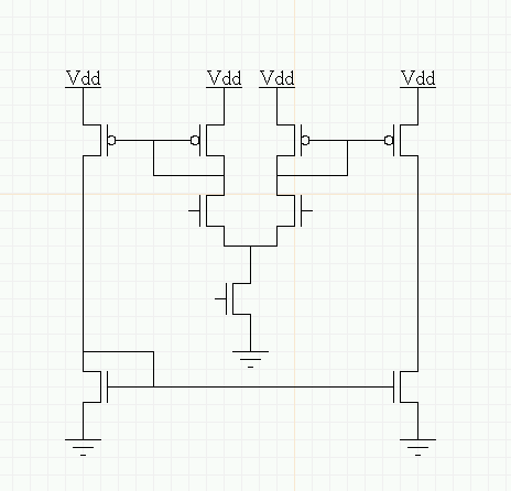
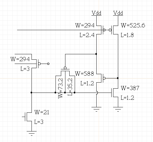
A transconductance amplifier, schematic drawing.
- Either drag the "dot" object from the library page or use the
period key (".") to place connections between the wires
at junctions. This is not strictly necessary, as xcircuit will
deduce connectivity from the T-connections of wires, not from
the "dot" symbols; it is merely a matter of preference depending
on the style with which you like to draw circuits. In the case
of wires crossing at a junction, the dot is necessary
since crossing wires generally do not indicate a connection in
schematic diagrams. You may also use a "jumper" object to
indicate that two crossing wires do not connect although this,
like the use of dots at T-junctions, is a matter of style and
personal preference.
- Add "circle" connections at the inputs and outputs. Once again,
this is a matter of style; the actual inputs and outputs from
the netlist's point of view will be indicated by pin labels
(see next step). The resulting diagram looks like the following:
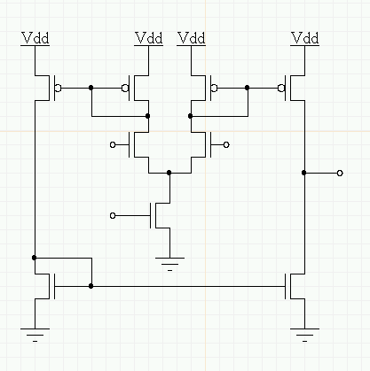
Same transconductance amplifier, a little fancier style.
- Because the amplifier will be a SPICE subcircuit, it is necessary
to tell the netlist generator where the input and output ports
are. For this, you need pin labels. Pin labels differ
from ordinary labels in several ways: By default, they are
colored red (though this can be changed), and are placed with a
slight offset from their marked positions, so the position
marker can be used as a tag to indicate what wire the label is
attached to. Additionally, the marked position is visible on
the drawing, since its exact location with respect to wires is
critical to the resultant netlist. Finally, pin labels only
appear on the top level of the hierarchy.
To generate the pin label, type key macro (capital) T, or
choose menu item "Netlist->Make Pin". Set justification as
desired and place the "x" marking the pin position over the
"o" of the circle objects, or on top of a wire. The pins in
this amplifier will be labeled "in.m", "in.p", "out", and "bias".
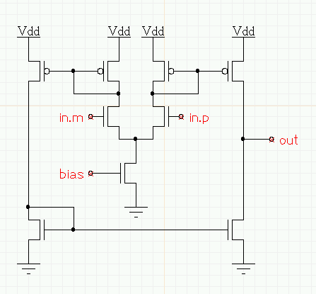
Transconductance amplifier with I/O pins marked.
- Now it's time to turn this schematic into a symbol, that is,
to make a symbol which will be used on the top-level drawing
to designate the transconductance amplifier. What we really
want to do is to use the symbol "wramp" (stands for "wide
range (transconductance) amplifier", which is what this is),
from library "avlsi.lps" (part of the distribution), as the
symbol for the schematic you just drew. Go to the built-in
library, then edit the "wramp" symbol from there by placing
the cursor over the "wramp" symbol and typing key macro
">". The result looks like this:
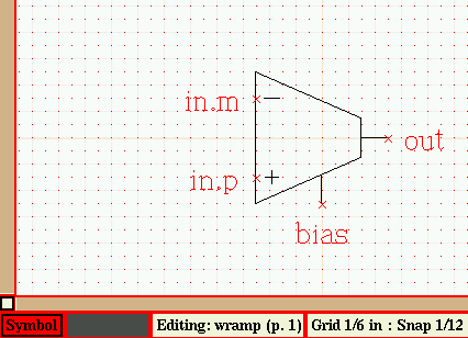
Transconductance amplifier symbol from the "avlsi.lps" library.
Note that in this picture, the bottom left-hand corner of
the screen says "Symbol" in the button that was, on Page 1, blank,
and the button that used to say "Schematic" is now blank. This
means that this object is a symbol, not a schematic, and it currently
does not have a schematic attached to it.
Also note that the pin labels marking input/output positions for
in.m,
in.p,
out, and
bias
are invisible on the library page, but become visible when
editing the object, that is, when the library object has been placed
on the top-level page. When the library object is used in a circuit,
the pin labels are again invisible. This way, the drawing doesn't
get cluttered up with nested labels.
- The procedure to attach the schematic to this symbol is quite
simple. Choose menu item Netlist->Associate With Schematic.
Immediately, you will be taken to the page directory, with the
message "Click on schematic page to associate." With the first
mouse button, click on Page 1 (assuming that's the amplifier
schematic). Instead of the usual behavior on the page directory
(go immediately to the page under the cursor), you will be
returned back to the amplifier symbol edit page.
Now both buttons appear at the same time, one named "Symbol" and
one named "Schematic". The one named "Schematic" is colored white,
indicated that the current page is the symbol, and that a
schematic exists which is the circuit represented by this symbol.
Press either button, and you will go to the schematic drawing
(back to Page 1). Press either button again, and you will return
to the symbol. The library object "wramp" is now a symbol for
the schematic of Page 1.
A symbol can be disassociated from its schematic, and
vice versa, by choosing menu item
"Netlist->Disassociate Symbol" or
"Netlist->Disassociate Schematic".
This menu option will appear only for the appropriate case.
Choose this action from the menu now. Note that the white button
in the lower left-hand corner goes back to being blank. The
library object "wramp" is no longer a symbol for the schematic
of Page 1.
Association can be initiated both ways. The alternate method is
as follows: Go back to Page 1 (the amplifier schematic).
Choose menu item "Netlist->Associate with Symbol" (note
that this is the same button that used to be "Disassociate").
You are transported to the library directory, with the instructions
in the message window to "click on the library page, then the
object to associate".
Click on the first library page (the one containing the wide-range
amplifier symbol "wramp"). Now click on the symbol "wramp".
Now, you will be returned to the original schematic page, and
once again, the buttons in the window's lower-left-hand corner
are red and white, indicating that you are on the schematic page
(red) but can move to the symbol page (white). Alternately to
clicking buttons to move between pages, you can choose menu
item "Netlist->Go To Symbol" (or "Go To Schematic",
as appropriate), or use the "/" key macro. Note that
the key macro only works if an association exists (i.e., it will
never create a new schematic or symbol, as described in the next
paragraph, although this was formerly the behavior in xcircuit
version 2.1(beta)).
The schematic and symbol both do not need to exist before association.
You can associate an existing schematic to a non-existing symbol
or associate an existing symbol to a non-existing schematic by using
the "Netlist->Make Matching Symbol" or
"Netlist->Make Matching Schematic" selection, respectively.
If you are editing a symbol, then you will be transported to the first
blank top-level page. If you are editing a schematic (top-level
page), a new User Library symbol will be generated and you will
be transported there. In either case, the new object will take
the name of its associated object, and all pin labels from the
original will be copied to the new, so that's one less step you
have to do yourself.
- Now it's time to use the symbol as a subcircuit in a top-level
circuit schematic. Go to Page 2, which will be the top-level
circuit. Draw an integrator as shown below:
Simple continuous-time integrator using a transconductance
amplifier.
Note that there is a "regular" text label titling the page;
this is made in the usual fashion, using key macro (lowercase)
"t", and therefore is not a pin label.
There is a one-to-one correspondence between the
pin labels on the schematic and the pin labels on the
corresponding symbol. This is important to make sure that
the wires attaching to the symbol on the top-level schematic
go to the correct destinations in the amplifier's schematic.
It is not an error to have unassigned pins: A pin inside
the schematic may be labeling a net for reference purposes
only. A pin on the symbol which is not used in the
schematic is much less likely, but may, for instance, be
representing an unconnected pin on an IC.
- Save this page. Call it "integrator". At this point, several
points should be noted:
- Two pages were saved instead of one. XCircuit followed
the path of the symbol to its schematic, and saved the
schematic for the amplifier. This becomes a separate
page in the PostScript output. Running "ghostview" or
your favorite PostScript previewer shows the two-page
output.
- Page 1, the page containing the schematic of the amplifier,
regardless of what you called it in the first place (if
anything), was renamed "wramp".
By convention, the schematic and symbol have the same
name, although this does not have to be the case.
- All the pages got saved as "Full Page" and not as
"Encapsulated". For multi-page files, "Encapsulated"
PostScript is not meaningful. Options for positioning
the schematic on the page will probably appear in the
future.
- Go to the top-level schematic page (Page 2, or "integrator").
From the menu, select "Netlist->Write Spice". The message
label will read "spice netlist saved as integrator.spc".
You can view the file integrator.spc
here. Note in particular that xcircuit has generated a
hierarchical netlist, using the amplifier "wramp" as a
subcircuit. The subcircuit contains parameters which are
its pin labels; the call to the subcircuit has parameters
which are the pin labels given on the top level page.
For reference, the resulting PostScript file can be found here:
integrator.ps
SPICE simulation: Xcircuit provides only the netlist. It can also
provide voltage sources and so forth, which will be described in the
next task. However, it has no concept of "models" and provides no
commands for running analyses. In the example above, the spice file
will need to be edited to insert models for devices "nmos" and "pmos",
Declare a voltage source and value for Vdd, and add commands
for DC operating point determination and transient analysis.
One thing you may have noticed about the previous circuit is that you
did not, in fact could not specify a value for the capacitor,
which defaulted in the spice netlist to 1.0pF. And there was no way
to specify a width and length of each nMOS and pMOS device. You might
have guessed: There does exist a way to pass values such as capacitance
to the capacitor object, and width and length to the MOS device objects.
Here's a brief description of how parameters work:
Each object contains a list of its parameters, NULL if there are no
parameters. Each item in this list declares what is the type of
parameter (so far, "string" or "integer", with only string types fully
supported at present), a default value for the parameter, and another
list which points to all the locations where the parameter gets
substituted.
It is important to keep in mind the distinction between an object
and its instantiations. If you are on Page 1 looking at an object
you just dragged back from the library, you are looking at a single
instance of that object. If you use the > key to
edit the object, then you are editing the object itself. Normally,
there is no particular need to make the distinction. However, when
using parameters, the object itself will declare the default parameter,
but each instance of the object may contain its own unique value for
that parameter.
Xcircuit adopts a method for editing parameters in which either the
default value or the instance value may be altered, and which one is
altered depends on what top-level page you came from. The
most obvious way to implement this is that if you edit an object from
one of the library pages, you are assumed to be altering the default
(the object on the library page always displays the default value of
all its parameters). If, instead, you edit the object by getting
there from a top-level page or another object, you are editing the
instance, and changes you make to the parameters will only
affect the value of that instance only. This should be made clear
by the tutorial below.
- Run xcircuit, which should automatically load "analoglib2.lps"
onto library page 2 (since xcircuit version 2.2.0. Otherwise,
load it from the subdirectory "examples" of the source
distribution).
- Go to library page 2 (macro L, click on second page).
You will see a set of
replacement objects for the basic circuit structures "capacitor",
"resistor", "nmos", etc. The main difference between these and
the original objects is that they contain labels indicating
values.
The parameterized analog component library.
- Select, say, the "Resistor" object and drag it back to Page 1.
- Copy the resistor so you have two resistors on Page 1.
- Edit one of the resistors (> key). You will note that,
in addition to pin labels, there are some other strings (called
"info labels") which will be described in detail later.
- Edit the string which reads "1.0 k(Ohm)" (e key macro, or
menu selection Edit->Edit). As you move the
cursor around the string, look at the message window. You will
note that in addition to the usual ASCII characters and string
commands such as font changes, half-space, etc., there is now
an additional embedded command label "Parameter(n)<
text>", where n is the parameter number, and
text is a substring (may be empty) which is the parameter
text. For the resistor, "1.0" is a parameter
describing the value, and "k" is a parameter for the metric
scale prefix. Unlike all other parts of the string, you cannot
delete the parameter delimiter marks (parameters must be
removed from a string with the "Unparameterize" function).
- Replace the substring "1.0" with "20" and replace "k" by "M"
or whatever your favorite resistor value is. Be sure that you
are inside the parameter delimiters when you make the change,
or you will get unexpected results.
- Pop back up to the originating page (< key). You will
see that only the resistor which you edited has its values
changed; the other one still has the original (default) values
of "1.0" and "k".
- Go to the library again (L key, then click on the second
page), and from there, edit the
resistor (> key). From here, change the value to, say,
"2.0 k". Note that now you are changing the default value,
not an instance value.
- Return to the library page (< key). Now the library
object shows the new resistance value, indicating that the
default value was altered. From here, go back to the
originating page (third mouse button). Now you see that the
resistor you altered retained its unique value, but the
resistor you didn't alter changed with the default.
The rule here is that each instance of an object accepts the
default unless is specifically declares its own unique value.
How does this work?
There are already traces of parameterization at work in xcircuit.
Each instance of an object has its own unique value for position,
rotation, color, and scale. These can be thought of as parameters.
Whenever xcircuit draws an object instance, it uses the unique
position, rotation, and scale to alter the 2-D transformation
matrix, then recursively calls the object drawing routine on the
object itself. When parameters are present, xcircuit first looks
up any unique values which the object instance might declare, and
substitutes these values into the object itself. If the instance
does not declare a particular parameter, then xcircuit substitutes
the default value. Then xcircuit recursively calls the drawing
routine on the object.
- Run xcircuit, as in the last example.
- Using the parameterized devices from the analoglib2
library, create the simple lowpass R-C filter shown below:
Simple R-C filter.
- Now, using what you learned from Task 4, alter the individual
parameter values so that they look like the following:
Simple R-C filter, with new parameter values.
- Choose menu item "File->Write XCircuit PS", and rename the top
page something obvious like "filter". Save it if you like.
- Choose menu item "Netlist->Write Spice".
You can view the resulting SPICE file
filter.spc here.
For reference, the finished PostScript file can be found here:
filter.ps
Although there are no MOS devices in this file, as in the previous task,
the SPICE deck will need to be completed with commands for performing
transient analysis and so forth, unless the file is to be used for
netlist comparison purposes only.
Spice output is determined solely by the ``info labels'' (which are green
by default, and only show up when the object they are in is on the top-level
page), in particular, those that begin with the token ``spice:''. There
are several ``escape sequences'' which have special meaning in this info
label. They begin with the ``%'' character and are summarized below.
Also, string parameters can be inserted directly into the info label, a
process which is described directly after.
Info label escape sequences:
- %%
- Inserts the character `%' into the netlist output line.
- ?
- When a single question mark is parameterized as its
own parameter, it is interpreted in the following way: If the
parser encounters a non-default value (i.e., a number), it uses
that number as the index. Otherwise, it generates a unique sequence
number for the object instance. This method is preferred over the
"%i" escape, as it allows each part number to be individually
assigned, if desired.
- (parameter)
- Any parameter may be inserted into the info
label, and therefore takes the value of either the instance string,
if defined, or else takes the value of the default string. The
question mark (?) is a special case (see above).
- %n
- Insert the name of the object.
- %p"name"
- Insert the name of a pin. The pin name must
be quoted exactly as is the label which defines the pin. The quotes
may be omitted if the name contains no white space and is followed
by white space (if in doubt, just use the quotes).
- %r
- Insert a carriage-return into the netlist output line.
Carriage-returns can also be inserted directly into the output
by using Alt-Enter or menu option
"Text->Insert->Carriage Return".
- %t
- Insert a tab into the netlist output line.
Obsoleted sequences (maintained for backward compatibility):
- %i
- Insert a number, in sequence, incrementing each time
a new object instance is visited during netlist compilation.
- %v"name"
- Insert the name of a parameter. The parameter
name must be quoted exactly as the label or label segement which
defines the default parameter. Alternately, a parameter
can be inserted directly into the string during text edit mode
using the "Alt-p" key. This is perhaps more intuitive, because the
value shown is either the default or substituted value, as appropriate,
rather than always listing the default value. The library file
analoglib1.lps,
which is available either
at this link or in the source distribution under the "examples"
directory, makes use of the "%v" method. analoglib2.lps
makes use of the direct-insertion method.
Example:
sim:n %pG %pS %pD
or:
spice:M%i %pD %pG %pS GND nmos
The top example produces an nMOS transistor line in a "sim" netlist, where
the actual net names inserted into the output file are those which correspond
to the gate, source, and drain pins, respectively. The bottom example does
the same thing for a SPICE netlist file, assuming that the SPICE model will
be called "nmos" (this can be parameterized if more than one model is
required; see paragraph below), and the "%i" sequence ensures that each
transistor gets a different label: M1, M2, M3, and so forth.
Inserting string parameters directly into a label:
While editing a label, use the key sequence ``Alt-p'' to insert a parameter.
If the object has only one parameter, it will be inserted automatically. If
the object has two or more parameters, xcircuit will prompt for the one to
use (listed by number). Once the copy of the parameter string is in the
label, there is effectively no difference between the copies: making changes
to one automatically changes the other (although the change may not show up
immediately). In general, this method is clearer than using ``%v'', since
the subsituted string appears directly in the info label rather than
referring back to the default string, so ``what you see is what you get.''
- From the default analog library (library page 1), grab the
(unparameterized) object "nmos" and drag
it back to page 1 (or whatever page you're working on).
- Edit the "nmos" object (key ">").
- Use the second mouse button to draw a selection box around the
word ``nmos'' in the first information (green) label.
- The word ``nmos'' will be highlighted; in this selection
mechanism, only that substring of the label has been selected.
- Choose menu option Text->Parameterize.
- Now edit the info label. When you get to the word ``nmos'',
you will notice, as printed in the message field at the bottom
of the xcircuit window, that it is bounded by invisible marker
characters ``Parameter(1)<'' and ``>''.
At this point, the SPICE model is a parameter of the object,
and its default value is ``nmos''.
- Because you entered the object from Page 1 rather than the Library,
what you are editing is the string instance, not the
string default. Change the parameter substring to read
nmos1, indicating an alternate MOS model called ``nmos1''
(which must be added to the output SPICE file before simulation!).
Make sure that the character "1" comes before the
">" parameter end marker; otherwise, it is not part of the
parameter, and instead becomes part of the default value.
- Finish editing and return to the calling page (key "<").
- Grab another object ``nmos'' from the library and place it on
Page 1. Edit it (key ">"). Note that the parameter
string contains the default value ``nmos''.
- Pop back out to Page 1 and run ``Netlist->Write spice''. The
resulting file is simple and can be included below.
Spice circuit Page 1
M1 net.1 net.2 net.3 GND nmos
M2 net.4 net.5 net.6 GND nmos1
.end
Information labels with embedded parameters are used in the library file
analoglib2.lps.
Note that in most objects
("Capacitor", "Resistor"), the parameterized value is in a string and
therefore shows up as part of the circuit diagram. However, others
("PNP", "NPN", where the SPICE model name is parameterized) have the
parameter only in an information label, where it does not show up on
the top-level page. Yet others ("nMOS", "pMOS") contain both (width
and length values appear on the top-level page and are copied into
the information label, but the name of the SPICE model only appears
in the information label).
As an addendum to this task, run xcircuit and load the file and generate
a spice circuit which uses two nMOS devices from the "analoglib2"
library page, each instance having a different SPICE model. In
addition, make the widths of the two devices different.
Note that when more than one string contain the same parameter, editing
one of the values will not be immediately reflected on the screen as
a change in the other(s). Popping back to the level above the object
and returning to edit the object will show all the proper substitutions.
All netlists generate output when they reach a ``fundamental'' object,
which is defined as an object containing one or more informational
labels.
Fundamental objects require several features:
- Fundamental objects are expected to be symbols. As in all
symbols, lines are interpreted as part of the symbol drawing,
not as nets. The only ``electrically relevant'' elements on
a symbol are the pins.
- Fundamental objects contain ``info labels'' which tell the
netlist compiler what to do with the information passed to
the object via the pins. Presently, there are three
different "styles" of netlist, named after the primary
format which uses that kind of netlist:
- Hierarchical, or ``spice'' netlists
- Flattened, or ``sim'' netlists
- Network, or ``pcb'' netlists
Information on each of these netlists is widely available
and distributed with layout and simulation software
packages. In a nutshell, however:
- Hierarchical and Flattened netlists both list by
element, with each line of the file consisting
of an element name followed by a list of network names
corresponding to each of the element's pins.
example:
Q1 net2 D0 gnd npn1
indicates that NPN transistor ``Q1'' has a collector
connection to "net2", base connection to "D0", and
an emitter connection to "gnd" (presumably a global
network).
- A Network netlist lists by network, with each
line consisting of a network name followed by a list
of pins in the circuit to which the network connects.
The element names are part of the pin names, with
the circuit hierarchy encoded in the element name by
slashes (`/'), much like a file system directory listing.
example:
Net3 control/74LS00_1#1-2 display/LED#2-5
indicates that the network named "Net3" connects
pin number 2 in the first 74LS00 chip in subcircuit
"control" to pin number 5 of the second LED in subcircuit
"display".
- A result of being an object and having an info-label is that the
"Symbol" button is green, indicating a "fundamental" element.
There is another type of symbol called a "trivial" symbol. This cannot be
designated from xcircuit. It is only a optimization which tells xcircuit
that an object does not produce output and is not a sub-schematic, and
therefore can be ignored except for the presence of pins. This prevents
the xcircuit netlist generator from wasting time looking for subschematics
or informational labels. Except for saving compute cycles, there is no
other difference between "trivial" and normal symbols. "Trivial" symbols
are declared in the PostScript file with a "% trivial" line.
A "subschematic" is a special kind of symbol which, unlike other symbols,
contains electrically relevant objects. Really, it's just a grouping of
electrical objects which bypasses the trouble of making a symbol to
represent the grouping. This can be useful, for instance, in drawing
one-half of a differential amplifier and repeating the schematic, flipped
horizontally.
XCircuit is extremely sophisticated in its ability to deal with subschematics.
It will determine how the subschematic is used, searching for input and
output "ports" that link the subschematic to the circuit on the level above.
The file in the xcircuit source "examples" directory
diffamp_test.ps is an example of such a file with subschematics.
It represents an obvious situation in which a subschematic is useful: This is
a differential amplifier, so a large portion of the amplifer is duplicated on
the positive and negative sides.
Differential amplifier sub-schematic: One half of an amplifier.
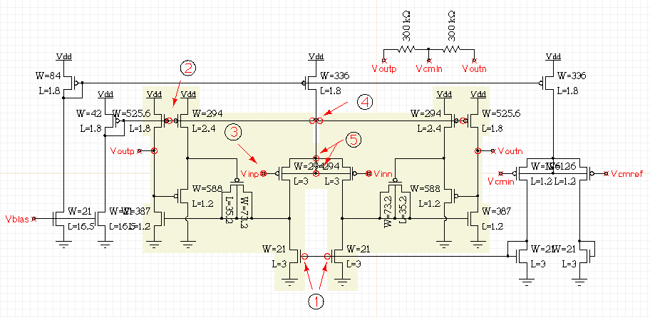
Differential amplifier complete schematic
The second of the two figures above shows how the half-amplifer subschematic
connects into the differential amplifier schematic. Note that no pins (pin
labels) have been explicitly called out in the subschematic. All connections
are determined from context. Different contexts which xcircuit finds and
interprets are marked with red circles on the differential schematic
(the unannotated version of the schematic can be
found here). The annotations, called out by number, are as follows:
- Port makes connection to a wire (polygon)
- Port makes connection on one side but not on the other
- Port makes connection to a label (pin)
- Port makes connection to a pin of another object
- Two ports in the subschematic get merged into one network
- (not shown) Port connects to port on another subschematic
On any given schematic page, port connections between symbols, between
subschematics, and from subschematics to symbols and vice versa, may be
from any layer in the circuit hierarchy to any other layer in the circuit
hierarchy.
XCircuit has the ability to highlight all wires belonging to a single
electrical network. This is a very useful feature for debugging
schematics, finding shorts and open-circuits. The command for
identifying network connectivity is menu selection
Netlist->Highlight Connectivity and the default key binding
for the same function is Alt-w. The key macro operates immediately
on either selected elements or whatever element is nearest the cursor,
while the menu item either operates immediately on any selected element
or prompts for a mouse click on an element to show connectivity for.
If multiple elements are selected prior to choosing the connectivity
function, connectivity will be searched for the first item encountered
in the select list which is part of a valid network.
As an example, load the file diffamp_test used previously in
Task 7 (examples/diffamp_test.ps in the XCircuit source
distribution). Place the pointer over any wire and type Alt-w.
The whole network will be ``highlighted'' in green. Note some features
of connectivity searches:
- Global networks such as ground have all parts of the network
highlighted, even if they are physically separated on the
drawing.
- Network selection is a different from element selection: It is
recursive. In the schematic drawing for "ampl_test" (Page 2),
networks inside the "half_amp" sub-schematic can be selected for
connectivity search, even though for purposes of normal move,
copy, etc., the "half_amp" can only be selected as an entire object.
- Pins can be selected as well as wires, and pins belonging to a
network will be highlighted along with the rest of the network.
- The name of the network is printed in the message window at the
bottom of the xcircuit screen. Hierarchy is relevant: A network
may have a different name depending on whether it is selected on
the top-level schematic, or somewhere down in the schematic
hierarchy. The network name displayed is that name belonging to
the network at the highest level of the hierarchy.
- Additional networks can be highlighted without erasing the original.
To erase one network before starting another, click the right
mouse button once ("Cancel" operation).
Currently, there is no method to detect and return a network name for
pin positions connecting two objects (that is, networks which do not
have a polygon or label explicitly attached to them in the schematic
drawing).
Note: Network connectivity searches only work as described above
in XCircuit version 2.3.5 rev. 1 and later.
File example "examples/logic8.ps" in the source distribution has
an example of a symbol on its own schematic. Run xcircuit on this example
file, and go to page 2, the schematic for the 2-input NAND gate. At the
bottom of the schematic is a picture of the "NAND" symbol. Note that
you can "push" (">" key) into the symbol picture, and then cross over
("/" key) to the schematic, returning to where you started in a circular
manner. You can do this all day until you run out of memory, so it is
not recommended. Fortunately, when xcircuit generates the circuit netlist,
it is not fooled into this recursive path. Instead, it detects the
presence of the recursion and will not treat the symbol picture as part
of the network. You can verify this by generating a SPICE netlist for
circuit "logic8" and reading the resulting file "logic.spc":
*SPICE circuit "logic" from XCircuit v2.30

.GLOBAL Vdd
.GLOBAL GND

.subckt invert Out In
M1 Out In Vdd Vdd pmos
M2 Out In GND GND nmos
.ends

.subckt nand Out In.1 In.2
M1 Out In.1 Vdd Vdd pmos
M2 Out In.1 ext13 GND nmos
M3 ext13 In.2 GND GND nmos
M4 Out In.2 Vdd Vdd pmos
.ends

X1 int1 Pin.1 invert
X2 Pin.4 int1 Pin.2 nand
X3 Pin.5 Pin.2 Pin.3 nand
.end
As you can see, the circuit has been created as intended, and the symbols
marked on their own schematics do not present a problem.
Caveat: It is possible to do more subtle forms of recursion. For
instance, in the "logic8" circuit, redraw the NAND2 schematic so
that the output goes through a buffer made of two inverters. This is
perfectly reasonable, by itself. Now, go to the inverter schematic, and
in place of the nMOS + pMOS stack, put a NAND2 gate with its two inputs
tied together between the In and Out pins. This is also perfectly reasonable,
by itself. However, the two changes taken together try to define the
NAND2 and inverter in terms of each other, which is recursive. Versions
of xcircuit before 2.3.5 rev. 1 will simply crash. Later versions will
detect the error as a suspiciously deep hierarchy, and halt the netlist
process before the processor hits a stack limit.
"sim" netlists are normally associated with digital VLSI circuits, but they
also can be useful for netlist comparisons of digital, analog, and mixed-signal
VLSI circuits. The standard "sim" format defines device types for nFET
(enhancement and depletion) and pFET transistors, resistors (explicitly
defined and lumped), and capacitors. However, the format has variously
been extended to cover other devices such as bipolar transistors, and any
variation of any component, provided it gets a unique letter assigned for
the device and is meaningful to whatever software uses the format downstream.
The main difference between "sim" and "SPICE" netlists is that SPICE allows
hierarchical descriptions containing subcircuits, whereas "sim" is by
definition a "flattened" version of a circuit. There is very little that
is necessary to say here, other than to note the ability of XCircuit to
generate flattened circuit netlists. XCircuit also has an option to
generate flattened SPICE. Note the difference in output, for instance,
between the output "logic.spc" for circuit "logic8" (shown in Task 9, above),
and the following output "logic.fspc" for the same circuit (generated by
Netlist->Write flattened SPICE:
*SPICE (flattened) circuit "logic" from XCircuit v2.30

M1 int1 Pin.1 Vdd Vdd pmos
M2 int1 Pin.1 GND GND nmos
M3 Pin.4 int1 Vdd Vdd pmos
M4 Pin.4 int1 nand1/ext13 GND nmos
M5 nand1/ext13 Pin.2 GND GND nmos
M6 Pin.4 Pin.2 Vdd Vdd pmos
M7 Pin.5 Pin.2 Vdd Vdd pmos
M8 Pin.5 Pin.2 nand2/ext13 GND nmos
M9 nand2/ext13 Pin.3 GND GND nmos
M10 Pin.5 Pin.3 Vdd Vdd pmos
XCircuit is ostensibly an ideal platform for generating schematic netlists
to compare against PCB (printed circuit board) designs. However, by
default (at least for now), xcircuit libraries are set up primarily for
VLSI layout work, so PCB netlisting requires a little extra work
(because a lot of users want to use XCircuit for PCB netlisting, I'd like
some help putting together libraries of IC's).
PCB netlists are fundamentally different from SPICE and sim netlists.
Instead of listing by device, the file lists by network.
The format is flattened, probably on the assumption that printed circuit
boards have no hierarchy. By default, xcircuit will list device pins
(network connections) by the name of the object followed by a dash and
the name of the pin to which the network connects. Any hierarchy present
in the xcircuit file is flattened by separating layers of the hierarchy
with slashes, as is done for the "sim" format.
For PCB symbols, the name of the object is used as the part name in the
netlist unless the object's symbol has a "pcb:" info label. In addition,
the sequence number of the part is assigned automatically unless declared
as a parameter in the "pcb:" info label. Typically, PCB components are
labeled "U" for integrated circuits, "R" for resistors, "C" for capacitors,
"J" for connectors and jumpers, and so forth. The sequence number for
each part, if automatically generated, will be unique with respect to
the name used for the part in the netlist output.
Consider Harry Eatons's ``LED'' design which comes as an example
in the "PCB" distribution. The relevant files are also linked
here:
- LED (a PCB-format file)
- LED.NET (a PCB netlist file)
Creating the schematic is very complicated, so I've done much of the
work to get you started. Here is an xcircuit file which can be used to
create a (partial, because it's unfinished) netlist to compare
against the LED printed circuit layout and netlist.
The important thing to notice about this file is the way components are
handled. Each component has an object name (a generic name, such as
"Resistor" or a part description, such as "LTC490"), text which may or
may not duplicate the title, and text which parameterizes the object
(such as resistor and capacitor values). In addition, each object is
parameterized for use in PCB. This requires a string inside the object,
an "info label" which is interpreted by the pcb netlist generator in
xcircuit. Also inside the object, not visible from the top level
drawing, are pin numbers for each object. For integrated circuits,
there is text on each pin which is a functional pin description.
This is not needed for the netlist, but makes it much easier to understand
the schematic.
- Start up xcircuit on the file FlareLED.ps.
- Go to the User Library (the library containing all of the ICs and
connectors in the schematic).
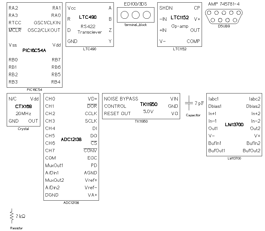
Integrated circuits and components library for FlareLED.
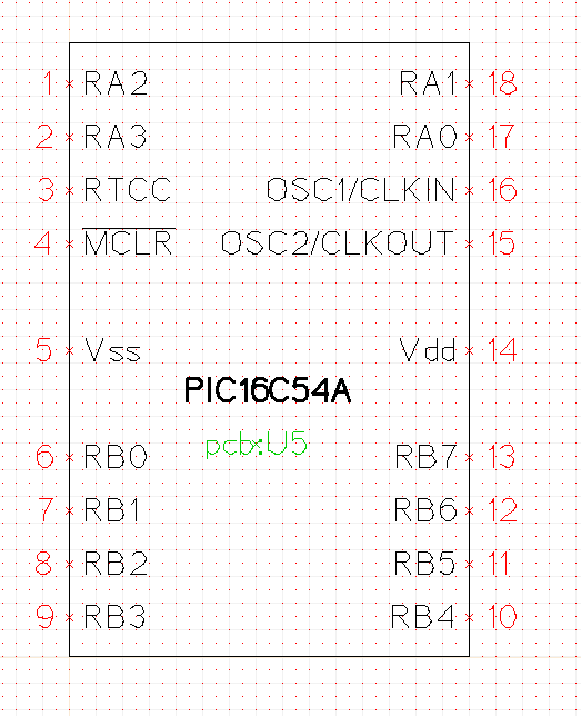
- Edit (">" key) the PIC controller (object named
"PIC16C54".
- You will note several things: This is an 18-pin chip, with pin
labels corresponding to the actual DIP package pin numbers.
Next to each pin number is the functional name for that pin.
On the top level page, only the functional names appear. On
the top level page, the device can be flipped, rotated, etc.,
without regard to the physical PCB layout. It is only necessary
that the networks of wires correctly connect the pins of
all the components.
- The "PIC16C54" object, like all the integrated circuits in the
schematic, has an "info label" which reads
pcb:U?
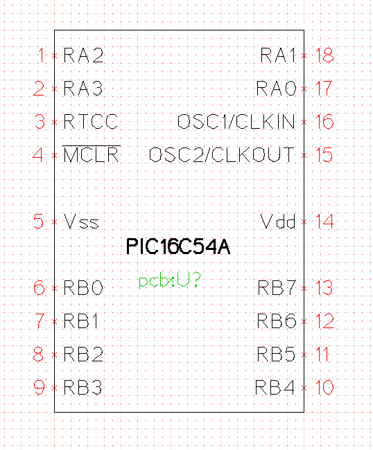
PIC 16C54 object, as edited from the library (default parameters)
- Edit this info label ("e" key). Note that the question
mark is a parameter.
- Escape from the label edit (3rd mouse button) and return to the
main page ("1" key). Now edit the same object,
the PIC16C54, from this page (">" key).
- Now you will see that the info label reads
pcb:U5
This is an instance value. It corresponds to the location
and label for an IC on the PCB layout.
PIC 16C54 instance, as edited from the top page (instanced parameters)
- End the label edit and return once again to the top level page.
From the menu, choose Netlist->Write pcb. The result
is a file named FlareLED.pcb. Compare this file to
the supplied netlist file named LED.NET. The XCircuit
schematic is not complete, but the parts that are correspond in
both netlist files.
- Challenge: Finish this schematic and show that the two
netlists are the same (``Layout vs. Schematic'', or ``LVS'').
- Another Challenge: Create an xcircuit library containing
the entire 7400 digital IC series and send it to me so I can
post it on this website.
Pins can be parameterized beginning in version 2.5.2 (it is allowed in
earlier versions but will cause invalid netlist output). Pins normally
work differently than label strings when making substitutions during
netlist generation; it is the network name which is substituted.
However, PCB-type netlists write pin names directly to the output, and
this is where parameterized pin names can be useful: For example, a
``quad part'' like a 7400 quad NAND chip has four NAND gates which are
identical except for their pin numbers on the package. Normally, a
PCB netlist would declare these as four parts, say, ``U1-1'' through
``U1-4''. By parameterizing all of the pin names, four instances can
be made representing the four gates inside the 7400 chip, each having
the correct pinout.
A method for saving the pinouts of gate subunits in chips was added
to version 2.5.2 along with the meaningful method for generating PCB
netlists from parameterized pin names. This method allows multiple
instances of a single object to appear on the same library page.
These copies should represent the object with different parameter
values. The most common use of this method is to parameterize pins
of a logic gate that is a subunit of a multiple-gate IC, and show
each of the subunits on the library page, where they can be used to
generate a PCB netlist.
Using XCircuit 2.5.2 or later, installed, start xcircuit and go to the
fourth library page ``Library: quadparts''. You will see the
following set of objects (partial view of the library):
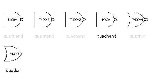
Partial view of the ``Quadparts'' library (from preliminary version).
Note that there are four copies of each named object. Each of the copies has
the same name, but three of the names are ``shaded out'' in a gray color.
The part with the name written in black is the original library part. It
contains parameters, but like standard library page objects, it displays all
of the default values for these parameters. As in Tasks 4 and 5, editing
parameter values in this library object will change the default values of
those parameters. The objects with the names printed in gray are
called ``virtual objects.'' They act like objects on a page rather than
objects in a library. Parameters in these objects may take on individual
values, and those specific values are copied along with the object when
it is selected and dragged back to a page.
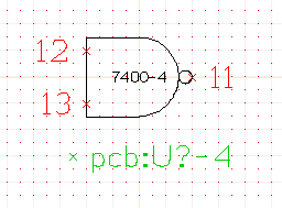
Editing a library virtual copy (instance) of gate ``quadnand''.
From the library page, grab all four ``quadnand'' objects and bring them
back to Page 1. With the four objects, one can make, for instance, a
delay flip-flop implementation from a single 7400 chip. This is shown
below:
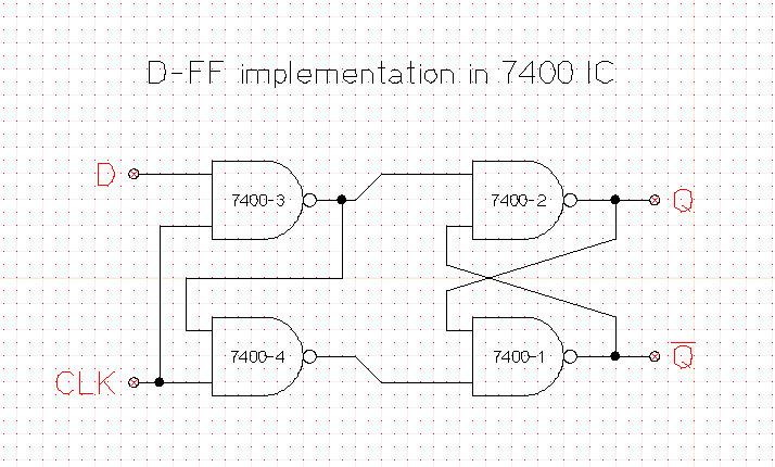
Delay Flip-Flop using the ``quadparts'' library.
After building the circuit, select Netlist->Write pcb. The
result is a valid PCB netlist for the circuit:
!Q          U2-2-5    U1-1-3
D           U3-3-9
CLK         U4-4-13   U3-3-10
int5        U4-4-12   U3-3-8    U2-2-4
int6        U4-4-11   U1-1-2
Q           U2-2-6    U1-1-1
The Python interpreter is supposed to make new netlist formats easy to
implement. However, the Python interface does not yet include access
to netlist information, so for the moment, netlist formats are limited.
As it stands, netlists must be one of three formats:
- Flattened ("sim" or SPICE)
- Hierarchical (with subcircuits in SPICE "subckt" format)
- Netlist (flattened, in a PCB netlist format)
Flattened netlists are the easiest to implement new formats in, since
the only structure in the file is determined by the elements themselves
(not counting comment lines, such as the first line that xcircuit writes
to the netlist file). The other two formats contain syntax that is
(currently) hard-coded into xcircuit (the "subckt" command in hierarchical
SPICE, and the entire syntax of PCB). Information about how to write
devices is encoded into ``informational labels'' (otherwise abbreviated
as ``info labels''). The syntax of info labels is described above in
Task 5.
Modifications to netlist formats can be useful in several ways:
- Implement a completely different netlist type (some subset of VHDL,
for instance)
- Modify an existing format (hspice or pspice syntax vs. ordinary
Berkeley spice3).
- Avoid explicitly drawing circuit schematics for simple devices.
- Write output at the gate level instead of the transistor level.
The last two require some explaining, so start up xcircuit and prepare
for another task.
Aggregate output per device
Here, we will change an "inverter" into a fundamental device consisting
of two transistors in the usual CMOS configuration for the inverter.
By default, XCircuit neither attaches schematics to gates nor defines
aggregate (multiple line) output for a gate because there are too many
ways to define a gate. For instance, the inverter could be an nMOS
device with a p-pullup, or it could be a bipolar-based TTL inverter,
etc., ad nauseum.
- Go to the first library page and drag back an inverter to the
first page.
- Add some pin labels to the input and output nodes. Call them,
say, "in" and "out" (or something less boring, if you prefer).
- Edit the inverter device (> key)
- Start an "info label" (I key, or Netlist->Make Info Pin
from the menu)
- Type
sim:n %pIn GND %pOut<Alt-Enter>p %pIn Vdd %pOut
where "<Alt-Enter>"
is the key combination Alt + Enter (also available using the
menu selection Text->Insert->Carriage Return).
Note that spaces, tabs, and other characters will transfer
to the netlist output, although embedded commands such as color,
font, and size change will not.
The embedded carriage return will end up in the netlist
output, as a real carriage return/newline. The result is shown
below.
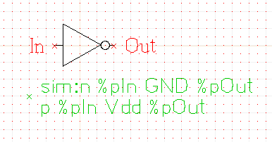
Inverter with informational label for "sim" netlist output.
- Return to the top level page, choose "File->Write Output" to
change the name from "Page 1" to something more useful.
Then, from the menu, select Netlist->Write sim.
The netlist output will look something like the following:
| sim circuit "aggregate" from XCircuit v2.30
n in GND out
p in Vdd out
- If you return to editing the symbol "invert", you will find
that after writing the netlist, the "Symbol" button in
the lower left-hand corner of the XCircuit window turned
green, indicating that this symbol is now considered to be
a "fundamental" object. That is, it has an informational
label and contains no subcircuits.
Output not on the device (transistor) level
Suppose, in the above example, we didn't know or care what is the
transistor-level implementation of the inverter, but wanted a SPICE
file showing the hierarchy, for which an inverter subcircuit could
be inserted at a later point.
- Repeat the above task through number 4.
- Write for the info label
spice:X%i %pIn %pOut inverter
- Return to the top level page, and write a SPICE netlist.
The netlist output will look something like the following:
*SPICE circuit "aggregate" from XCircuit v2.30

X1 in out inverter
.end
- While this deck is not directly simulatable, it only awaits the
insertion of an inverter model in the form of a subcircuit.
This task will summarize most of what has been covered above in the tutorial
with a practical example, a power supply bridge rectifier for a printed circuit
board layout. The example will work through detailed explanations of each
step, for the benefit of the impatient.
The bridge rectifier is a simple power supply circuit which transforms an AC
supply (e.g., wall outlet) into a DC current for powering a circuit. The
"bridge" is a diode bridge, a loop of four diodes which act as a full-wave
rectifier. The bridge also acts as a nonlinear resistance in a simple
single-pole R-C low-pass filter. The filter pole is set by a large
polarized capacitor on the rectifier output. The larger the capacitor,
the steadier the output voltage, including resistance to short spikes and
dropouts of the AC supply.
Usually the bridge rectifier circuit drives the input of a voltage regulator
to clean up the 120Hz bumps generated by the less-than-ideal lowpass filter,
and to adjust the voltage between the transformer and the circuit being
powered. For simplicity, this example will not consider the voltage
regulator.
For more information about bridge rectifiers, see Horowitz and Hill,
The Art of Electronics, 2nd edition, pages 45 and following
(Cambridge Press, 1989).
Step 1
If you have xcircuit version 2.3.3 after revision 6, there will be a
symbol "Diode" (with capital-D) in the analoglib2.lps file (the
second library page). If not, you can update your library from this
link: analoglib2.lps,
and skip to Step 2. Alternatively, you can
use the following instructions to generate the PCB-compatible diode
from the simple diode on the first library page (named "diode", no
capital letter).
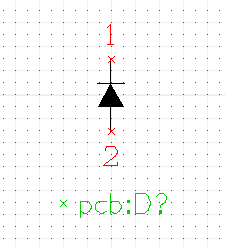
The diode symbol "diode" in the first library is not configured for use in
PCBs. This can be changed easily. Go to the first library page (l
key macro), and edit the diode symbol (> key macro).
Change the pin names to "1" and "2" (edit, or e key) to match
PCB naming conventions. Finally, add an "info label" for the PCB
netlister (I key, or else create a normal label then select
menu item Netlist->Convert Label To...->Info label). The label
text should be
pcb:D?
After creating the label, use the second mouse button to drag a select
box over the question mark. Only the question mark should be highlighted.
Then select menu item Text->Parameterize. As described earlier in
the tutorial, the PCB netlister will use this parameterized string to
determine a part number for the diode, or else the part number can be
explicitly declared by editing the info label from each of the four
instances of symbol "diode" that we will generate.
Return to a drawing page (< key, 1 key to go to Page 1)
and continue with Step 2.
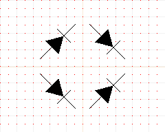
Step 2
Go to the library (l key, twice to get to the analoglib2 page,
or once if using an edited version of the simple diode, from Step 1)
and select the diode for copying (c key).
This action will take you back to the main
drawing page, with a diode instance in tow. While the diode is still
selected, rotate it (r key, as many times as necessary).
Place it four times with a click of the first (left) mouse button,
and finish with a click of the third (right) mouse button. Rotate and
position the diodes as shown below.
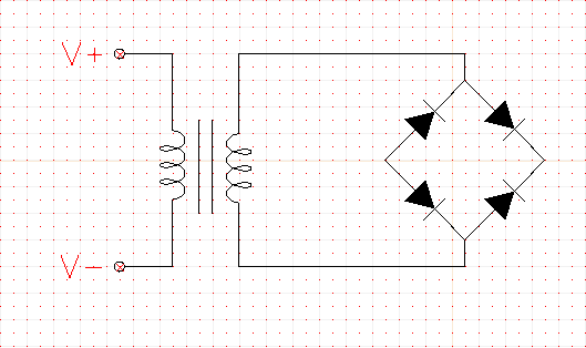
Step 3
Connect the diodes together in a bridge configuration. While the
diode endpoints are not quite on the drawing grid when the diode is
rotated 45 degrees, they are fairly close (as drawn, see figure
above), and there is some "slop" in the netlist generator when
considering whether two wires are connected together. No special
measures are necessary to ensure the connection.
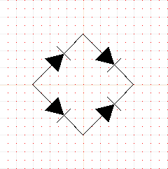
Make a schematic out of the rectifier by selecting all the components
drawn so far, typing m to "make" the object, and name
the object "rectifier". This is a "subschematic", as described
above in the tutorial, and pins will be determined from context.
Step 4
Grab the transformer symbol from the "analoglib2" library (2nd library
page). Add wires to the transformer input, ending in terminals for
the input AC supply. Name these terminals "V+" and "V-" (typographical
suggestion: use the Symbol font for "+" and "-").
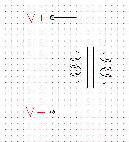
Connect the transformer and the rectifier together as shown.
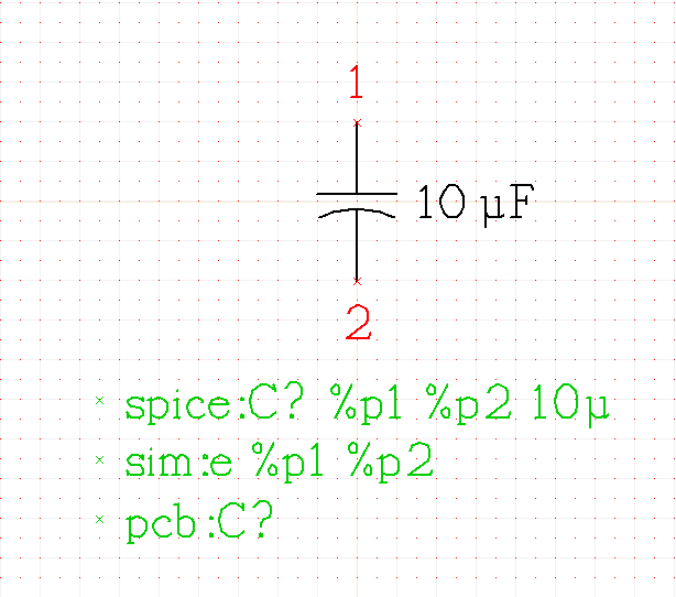
Step 5
Grab two capacitors (one polarized, one not) from the second library
page. These are the capacitors with values listed.
They are already configured for use with a PCB netlist.
The capacitors default to a picofarad value (for use with VLSI
layouts, not PCBs), so the value string needs to be edited to
change this to the "micro" symbol for microFarads.
Typographical note:
The best way to do this is to change the font of the whole
string from "Times-Roman" to "Times-RomanISO" (use menu option
Text->Encoding->ISO-Latin1 or, while editing the label,
use the Alt-e key combination). The "micro"
symbol (Greek "mu") is available from the font symbol table (accessed
with the backslash key while editing text). The change to ISO
encoding will be necessary on both the value string and the "SPICE"
info label.
Netlist note:
The SPICE netlist generator will convert the "mu" symbol to the "u"
used by SPICE. This happens regardless of whether the ISO-encoded
"mu" or the Symbol font "mu" is used. Of course, one may also
write ASCII "u" in the value string.
Step 6
Connect all the parts together on the top level page as shown.
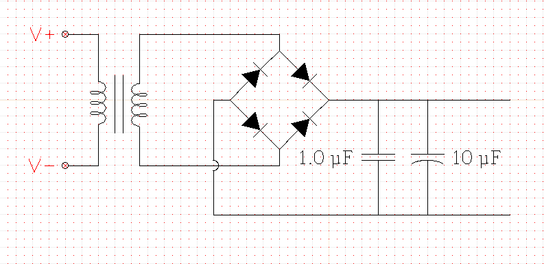
Add finishing touches, and the completed bridge rectifier should
look something like the one shown below.
The xcircuit file can be obtained here: bridge.ps.
Step 7
Select menu option File->Write XCircuit PS and select a "Page label"
for the file. This will be the name used by the netlist generator for
the netlist file name.
Generate the PCB netlist by selecting menu option Netlist->Write pcb.
The result is shown below:
   V-          T1-2
   V+          T1-1
   int5        T1-3   rectifier1/D4-1   rectifier1/D3-2
   int6        T1-4   rectifier1/D2-1   rectifier1/D1-2
   Vout        rectifier1/D3-1   rectifier1/D1-1   C2-1   C1-1
   GND         rectifier1/D4-2   rectifier1/D2-2   C2-2   C1-2
and can also be obtained from this link:
bridge.pcb.
Step 8
The example is essentially done, but we can take it one step further
by generating a symbol called "power_supply" to represent this circuit
in a larger schematic.
Go to an empty page (Page 2, perhaps) and generate the following figure:
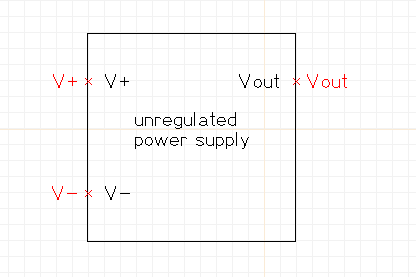
Labels in black are normal text (created with the t key), and labels
in red are pins (created with the T key). After drawing, select
everything and put it all into an object (m key). Name the object
"power_supply".
Step 9
Now go back to Page 1, the bridge rectifier schematic. Choose the menu
selection Netlist->Associate with Symbol. You will be taken to
the library directory. Click (once) on the user library. You will be
taken directly to the user library. Finally, click (once) on the symbol
"power_supply". Now you should be returned to the bridge rectifier
schematic, with the difference that there is a white button labeled
"Symbol" in the bottom left-hand corner of the window. Clicking on the
button toggles the drawing window between the schematic and its
(newly associated) symbol.
Step 10
Return to Page 2, the top-level schematic with the "power_supply" symbol.
Try out the following (trivial to the point of uselessness) circuit
(also available at this link: powersup.ps):
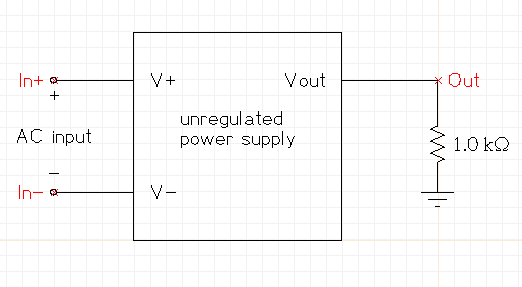
Go to menu selection File->Write XCircuit PS and rename the "Page
label" to "powersup". Then select Netlist->Write pcb to
generate a new PCB netlist.
Now look at the result:
   NET1        power_supply1/T1-3   power_supply1/rectifier1/D4-1   \
              power_supply1/rectifier1/D3-2
   NET2        power_supply1/T1-4   power_supply1/rectifier1/D2-1   \
              power_supply1/rectifier1/D1-2
   In+         power_supply1/T1-1
   In-         power_supply1/T1-2
   Out         power_supply1/rectifier1/D3-1   power_supply1/rectifier1/D1-1   \
              power_supply1/C2-1   power_supply1/C1-1   R1-1
   GND         power_supply1/rectifier1/D4-2   power_supply1/rectifier1/D2-2   \
              power_supply1/C2-2   power_supply1/C1-2   R1-2
which can also be obtained from this link:
powersup.pcb.
Note that the main difference is that the netlist is hierarchical, with
components inside the power supply being referenced by the prepended
name "power_supply1". The resistor, the only component on the top-level
page, is not so prefixed. Throughout the netlist, net names take the
name given in the highest level of the hierarchy.
 Back to the xcircuit home page. . .

email: tim@bach.ece.jhu.edu